Thyristor Daya Tinggi Promosi untuk Kontrol Fase
dapatkan harga terbaru| Jenis pembayaran: | L/C,T/T,Paypal |
| Inkoterm: | FOB,CFR,CIF |
| Transportasi: | Ocean,Air |
| Pelabuhan: | Shanghai |

| Jenis pembayaran: | L/C,T/T,Paypal |
| Inkoterm: | FOB,CFR,CIF |
| Transportasi: | Ocean,Air |
| Pelabuhan: | Shanghai |
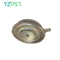
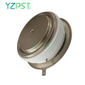
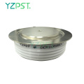
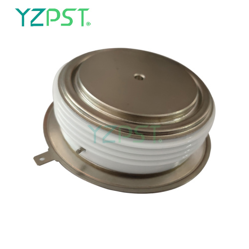
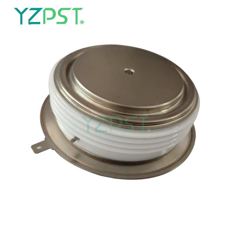
Model No: YZPST-R219CH12FN0
Merek: YZPST
Thyristor Daya Tinggi untuk Kontrol Fase
YZPST-R219CH12FN0
Fitur:
.Guaranteed Maximum Turn-Off Time
. Semua Struktur Tersebar
. Perangkat Rakitan Tekanan
. Konfigurasi Gerbang Penguatan Digigit
. Kemampuan dV / dt tinggi
KARAKTERISTIK LISTRIK DAN PERINGKAT
Blocking - Off State
|
|
|
VRRM (1) |
VDRM (1) |
VRSM (1) |
|
1200 |
1200 |
1300 |
V RRM = Tegangan balik puncak berulang
V DRM = Puncak tegangan kondisi mati berulang
V RSM = Tegangan balik puncak tidak berulang (2)
|
Repetitive peak reverse leakage and off state leakage |
IRRM / IDRM |
15 mA 70 mA (3) |
|
Critical rate of voltage rise |
dV/dt (4) |
200 V/msec |
Catatan:
Semua peringkat ditentukan untuk Tj = 25 o C kecuali dinyatakan lain.
(1) Semua peringkat tegangan ditentukan untuk diterapkan
50Hz / 60zHz bentuk gelombang sinusoidal di atas
kisaran suhu -40 hingga +125 o C.
(2) 10 msec. maks. lebar pulsa
(3) Nilai maksimum untuk Tj = 125 o C.
(4) Nilai minimum untuk bentuk gelombang linear dan eksponensial hingga 80% berperingkat V DRM . Gerbang terbuka. Tj = 125 o C.
(5) Nilai tidak berulang.
(6) Nilai di / dt ditetapkan sesuai dengan EIA / NIMA Standard RS-397, Bagian 5-2-2-6. Nilai yang ditentukan akan menjadi tambahan dari yang diperoleh dari sirkuit ubber, terdiri dari kapasitor 0,2 m F dan 20 ohmresistensi secara paralel dengan thristor yang diuji.
Melakukan - pada negara
|
Parameter |
Symbol |
Min. |
Max. |
Typ. |
Units |
Conditions |
|
Max. average value of on-state current |
IT(AV)M |
|
929 |
|
A |
Sinewave,180o conduction,Tc=55oC |
|
RMS value of on-state current |
IT(RMS)m |
|
1893 |
|
A |
Nominal value |
|
Peak one cPSTCle surge (non repetitive) current |
ITSM |
|
-
9.0 |
|
kA
kA |
8.3 msec (60Hz), sinusoidal wave- shape, 180o conduction, Tj = 125 oC 10.0 msec (50Hz), sinusoidal wave- shape, 180o conduction, Tj = 125 oC |
|
I square t |
I2t |
|
405x103 |
|
A2s |
8.3 msec |
|
Latching current |
IL |
|
- |
|
mA |
VD = 24 V; RL= 12 ohms |
|
Holding current |
IH |
|
1000 |
|
mA |
VD = 24 V; I = 2.5 A |
|
Peak on-state voltage |
VTM |
|
2.04 |
|
V |
ITM = 1400 A |
|
Critical rate of rise of on-state current (5, 6) |
di/dt |
|
1500 |
|
A/ms |
Switching from VDRM £ 1000 V, non-repetitive |
|
Critical rate of rise of on-state current (6) |
di/dt |
|
1000 |
|
A/ms |
Switching from VDRM £ 1000 V |
Gating
|
Parameter |
Symbol |
Min. |
Max. |
Typ. |
Units |
Conditions |
|
Peak gate power dissipation |
PGM |
|
30 |
|
W |
|
|
Average gate power dissipation |
PG(AV) |
|
2 |
|
W |
|
|
Peak gate current |
IGM |
|
- |
|
A |
|
|
Gate current required to trigger all units |
IGT |
|
300 |
|
mA |
VD = 10 V;IT=3A;Tj = +25 oC
|
|
Gate voltage required to trigger all units
|
VGT |
|
3.0 |
|
V
|
VD = 10 V;IT=3A;Tj = +25 oC
|
|
Peak negative voltage |
VRGM |
|
5 |
|
V |
|
Dinamis
|
Parameter |
Symbol |
Min. |
Max. |
Typ. |
Units |
Conditions |
|
Delay time |
tgd |
|
1.0 |
- |
ms |
VD=67% VDRM, IT=2000A, di/dt=60A/us, IFG=2A, tr=0.5us, Tj=25C |
|
Turn-on time |
tgt |
|
2.0 |
- |
|
|
|
Turn-off time (with VR = -5 V) |
tq |
- |
- |
10 |
ms |
ITM=1000A, tp=1000us, di/dt=60A/us, Vr=50V, Vdr=33%VDRM, dVdr/dt=200V/us |
|
Reverse recovery current |
Irm |
|
- |
|
A |
ITM=4000A, tp=2000us, di/dt=60A/us |


Tel: 86-514-87782298
Whatsapp: +8613805278321
Alamat: 3rd Floor, Weiheng Building No.20 B Area, Yangzhou, Jiangsu China
Situs web: https://id.yzpst.com


Privacy statement: Your privacy is very important to Us. Our company promises not to disclose your personal information to any external company with out your explicit permission.
Fill in more information so that we can get in touch with you faster
Privacy statement: Your privacy is very important to Us. Our company promises not to disclose your personal information to any external company with out your explicit permission.